Beryllium X-Ray Window Assembles
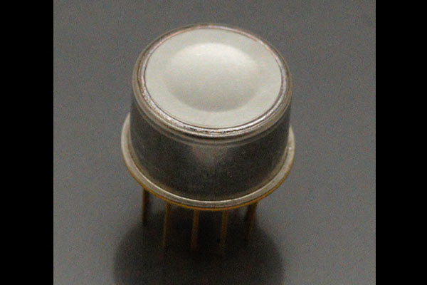
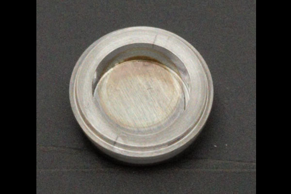
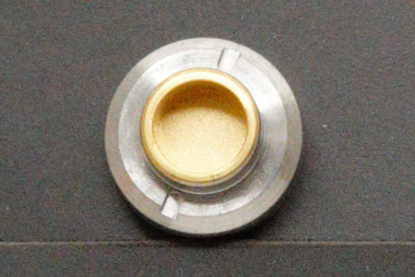
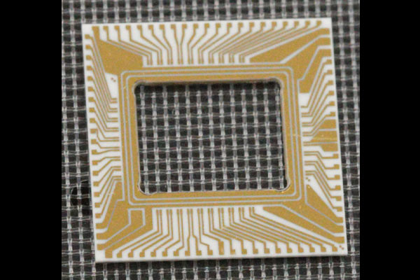
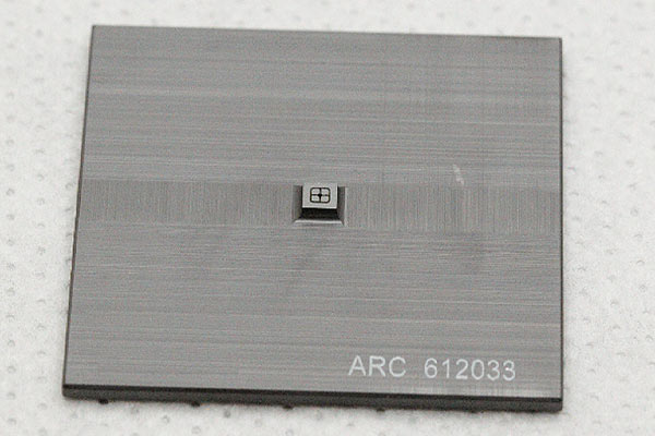
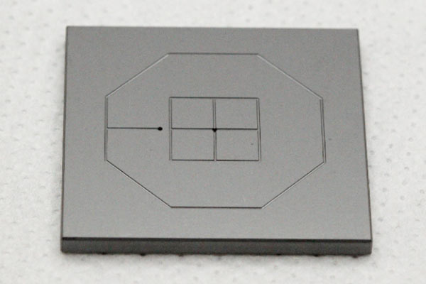
Arcnano specializes in the assembly and production of beryllium windows for x-rays and scientific instruments. This specialty includes both the sources and detectors.
Arcnano performs disk singulation and leak testing from customer provided foils. In addition, we braze, solder reflow, deposit thin films, passivate and helium leak check the windows.
In the near future, Arcnano will be performing rolling mill operations of Beryllium sheets down to 125 um and above for X-ray source windows, and from 12.7 microns and above for X-ray detector windows.
Thicker “bulk” windows are in production at Arcnano, typically in the few mm range.
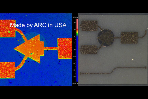
Thin Film, MEMs, Wafer Scale Devices
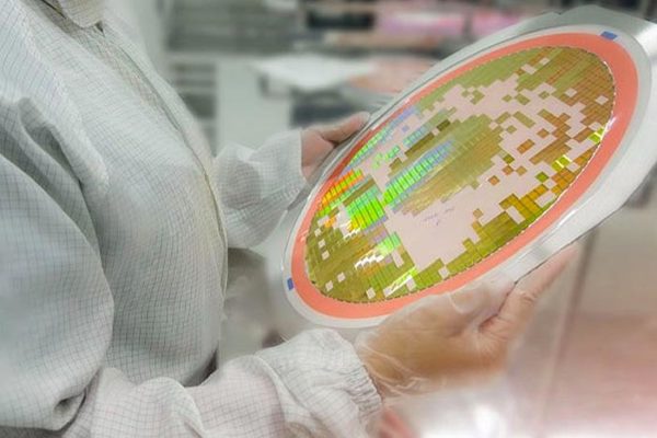
Our Thin Film and full MEMs level Wafer Fab provides contract manufacturing ranging from FEOL to BEOL operations.
Process Development to Full Wafer Scale Device Fabrication
Mask Design to GDS2 Files
Deposition, Photo, Etch, Dice, Test
Wafer Chucks
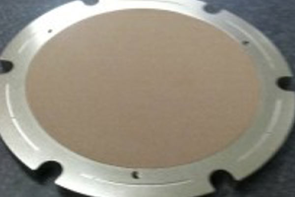
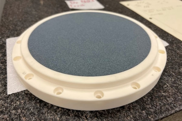
Arcnano manufactures both OEM reaplcement and custom wafer chucks in porous ceramic, stainless steel, Ni plated copper and other materials.
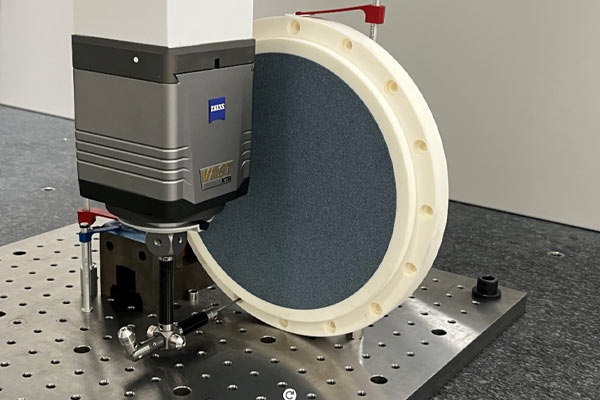
We achieve < 2um flatness and parallelism over 150mm and < 8um over 300mm.
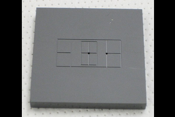
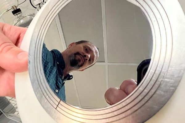
6” Arcnano model of vacuum chuck (generic) with vacuum attach
SiC Vacuum Chucks
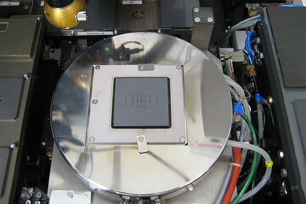
Arcnano manufacturers SiC Vacuum Chucks for Infra Red Focal Plane Array hybridization process where the ROIC chip is bonding to the detector chip.
Most of these chucks are for FC-150 and FC-300 device hybridization tools made by SET in France, formerly a division of Suss Microtec.
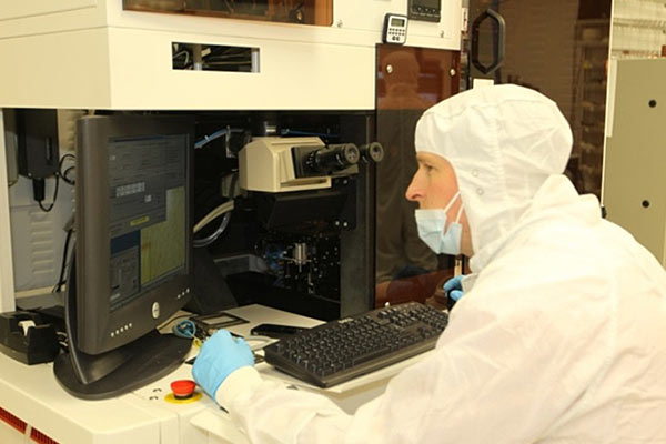
We supply chucks with sub micron flatness and parallelism. We use a Tropel Flatmaster for measurement of flatness and a Zygo NexView for measurement of surface roughness.
3D Chip Stacking, Hybridization, Indium Bumping
3D Chip Stacks are vertical laminations of one chip upon another chip with electrical connectivity. Often referred to as hybridization, pioneered for Infra-Red Focal Plane Arrays (IR FPAs), this allows for a read-out IC (ROIC), typically CMOS, to be bonded to a compound semiconductor 2-D detector or emitter array.
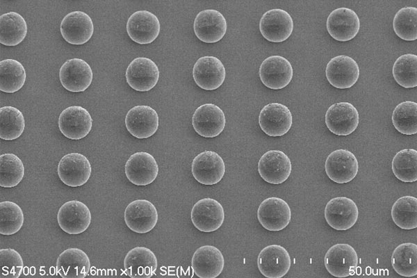
Arcnano specializes in IR FPAs, high power laser diodes, avalanche photo diodes or Si chip-on-chip. We perform backend processing including contact metallization, indium bumping, die singulation, hybridization and packaging.
Arcnano makes its own SiC vacuum chucks, in-house, and also for much of the industry.
Wafer Thinning and Dicing
Arcnano’s Disco Hi-Tech wafer dicing saws have higher power spindles which can easily dice ceramics, such as Alumina, as well as various semiconductor wafers. Arcnano thins and dices up to 300 mm wafers.
Compound Semiconductor Device Wafers. Arcnano specializes in compound semiconductor substrates such as SiC, GaN, Indium Phosphide (InP), Gallium Antimonide (GaSb) and others. Backside grinding, thinning, lapping and polishing are performed on a regular basis.
Single Point Diamond processing is in our future plans.
