3D Chip Stacking, Hybridization, Indium Bumping
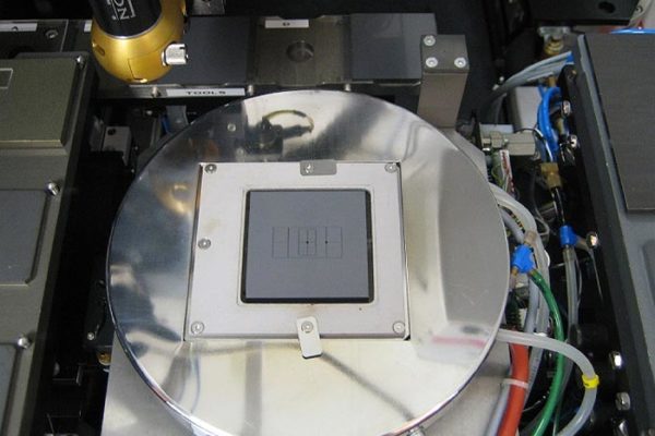
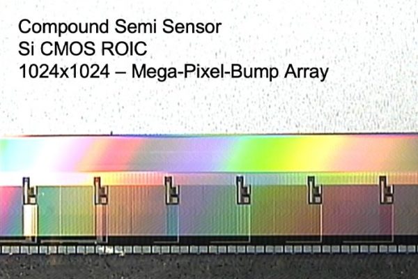
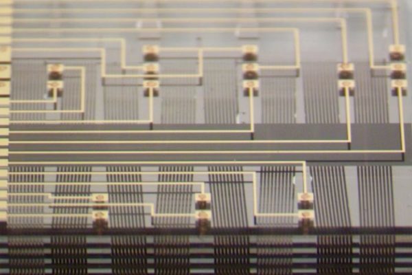
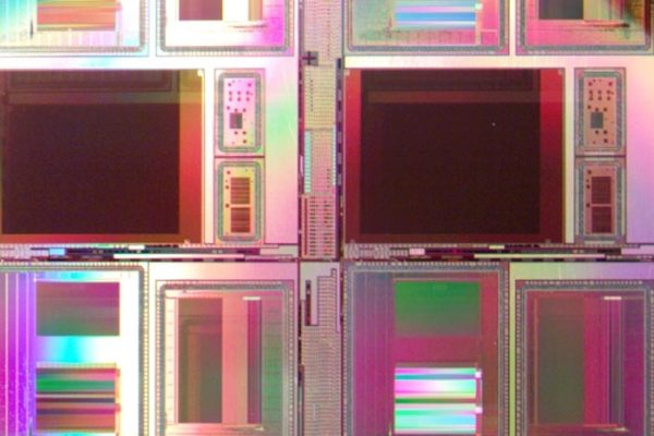
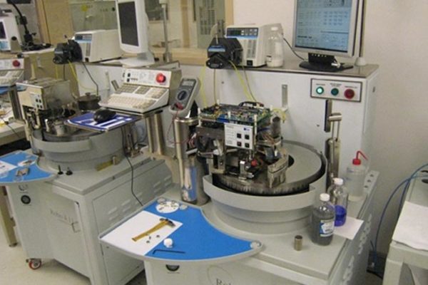
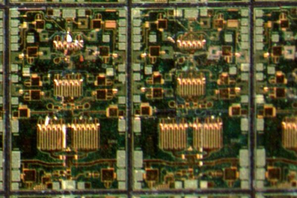
3D Chip Stacks are vertical laminations of one chip upon another chip with electrical connectivity. Often referred to as hybridization, pioneered for Infra-Red Focal Plane Arrays (IR FPAs), this allows for a read-out IC (ROIC), typically CMOS, to be bonded to a compound semiconductor 2-D detector or emitter array.
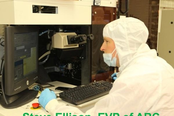
Arcnano specializes in IR FPAs, high power laser diodes, avalanche photo diodes or Si chip-on-chip. We perform backend processing including contact metallization, indium bumping, die singulation, hybridization and packaging.
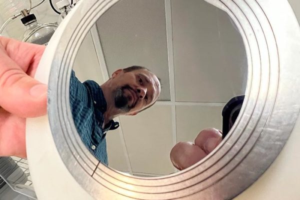
Arcnano makes its own SiC vacuum chucks, in-house, and also for much of the industry.
MEMs, Sensors, Thin Film Devices
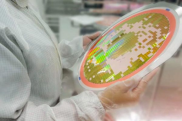
Arcnano provides semiconductor micro-fabrication services across a wide variety of areas, from blanket thin film coatings, including precision multilayer coatings, to fully patterned multilayer completed devices. Completed work can be delivered at any stage, ranging from wafer level to fully packaged and tested chips.
MEMs (micro electro-mechanical systems), flow sensors, oscillators, magnetic devices, and spectrometers.
Deposition, Photolithography, Etch Operations
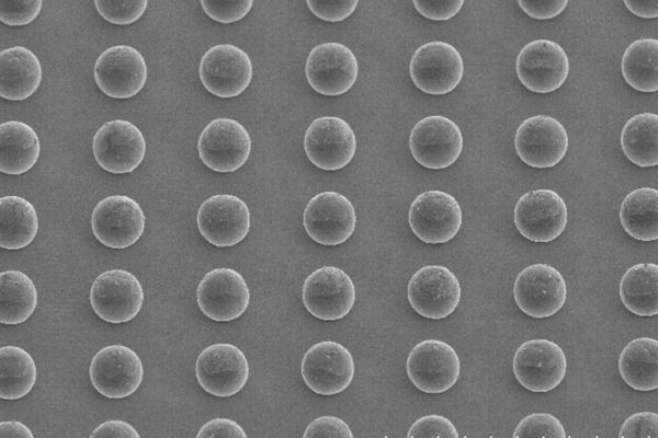
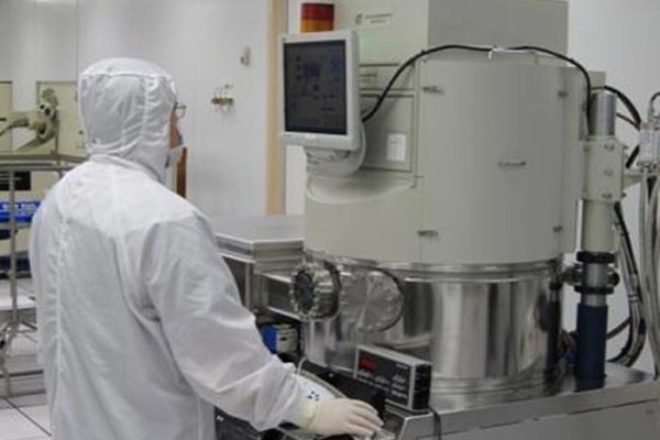
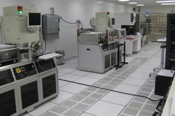
Thin film deposition processes include Sputtering, Evaporation, CVD, LPCVD and ALD. Arcnano has over 100 sputtering targets and is expert at metallization, dielectrics, and magnetic thin films. Indium Bumping for 3D Chip stacking is accomplished in a dedicated Indium evaporation system.
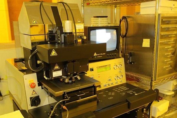
Arcnano’s photo patterning consists of Suss MA/BA 6 with 1 um line widths as the minimum feature size. This capability is extended with Cannon and GCA steppers into the 250 nm feature size range.
Our standard etching processes include wet etching, Ion Milling, RIE, and DRIE.
Wafer Grinding, Lapping, & Polishing
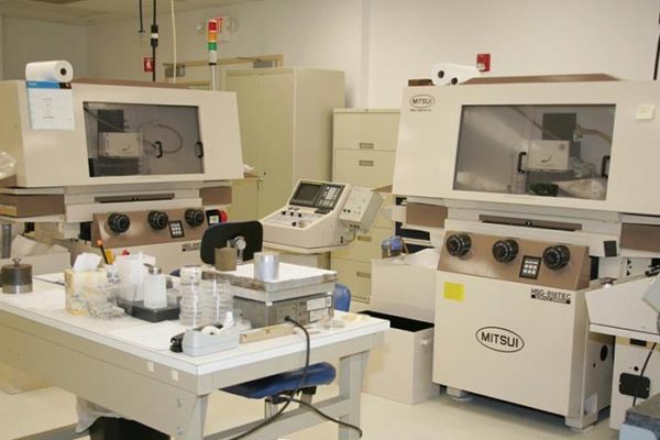
Arcnano provides backside grinding, lapping and polishing services to meet our customers needs. Our CNC Surface Grinders, fitted with air bearing spindles, are used for grinding metals and ceramics, such as Alumina and Silicon Carbide. This grinding expertise is complimented by lapping and polishing machines ranging from 12 to 48 inches in diameter.
Additionally, Arcnano provides backside grinding services, thinning, lapping and polishing for compound semiconductor substrates such as SiC, GaN, Indium Phosphide (InP), Gallium Antimonide (GaSb) and others.
- Air Bearing Spindles
- CNC Grinders
- Lapping
- Polishing
Wafer Dicing
Semiconductor Back End Fabrication is a specialty at Arcnano.
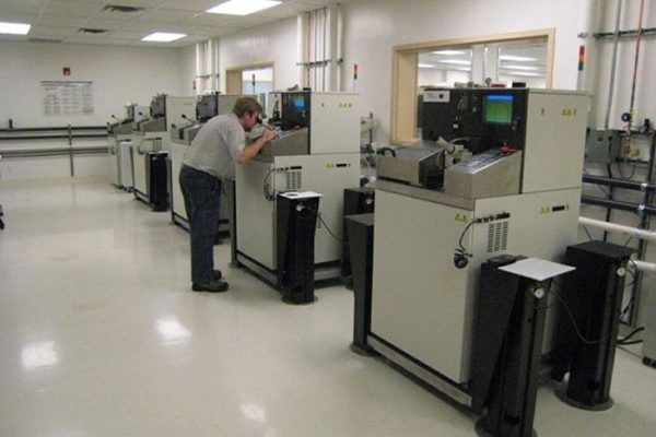
Arcnano’s Disco Hi-Tech wafer dicing saws have higher power spindles which can easily dice ceramics, such as Alumina, as well as various semiconductor wafers. Arcnano thins and dices up to 200 mm wafers.
Additionally, Arcnano has expertise with special applications with SOI, ceramic, glass and other materials.
- Silicon
- Compound Semi
- Ceramics
- Glass
